Scaling Precision: The Technology Enabling Ultra-Large OLED Displays and Next-Gen Semiconductors
Ganesh Babu Chandrasekaran's innovations in CVD and PECVD chambers have enabled the production of ultra-large OLED displays and advanced semiconductor devices. His contributions include patented technologies that improve plasma uniformity, thermal stability, and mechanical alignment.
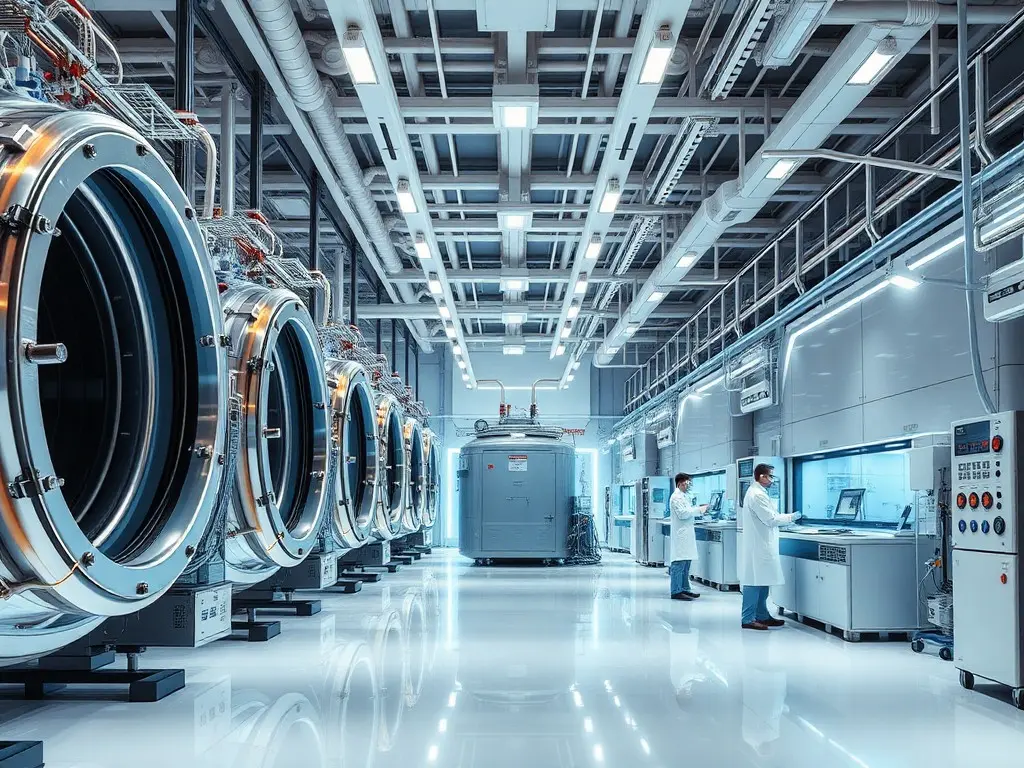
The production of ultra-large OLED displays and advanced semiconductor devices relies on advanced Chemical Vapor Deposition (CVD) and Plasma-Enhanced Chemical Vapor Deposition (PECVD) chambers. Ganesh Babu Chandrasekaran has contributed to the design and commercialization of multiple generations of CVD and PECVD chambers. His innovations include a Power-Efficiency (PE) diffuser that improves plasma distribution and a Flat Head Ball (FHB) alignment unit that increases alignment accuracy. These technologies have enabled the production of Gen10.5 substrates up to 3000 × 3420 mm, representing a 30–40 percent size increase over previous generations. Chandrasekaran's work has supported the release of large-area CVD platforms for advanced thin-film transistor applications. His patented technologies are deployed in high-volume manufacturing environments, improving yield performance and reducing defectivity.
This content was automatically generated and/or translated by AI. It may contain inaccuracies. Please refer to the original sources for verification.